Photonic silicon components are huge compared to their electronic counterparts, and this precludes their use in processors which, as you know, work with nanoscale-sized transistors for now. This creates considerable additional difficulties and costs, but researchers at the University of Toronto in the United States and ARM itself believe they can significantly reduce these problems.
Plasmonics, or how to connect processors using light beams
The fact that silicon photonic components are much larger than electronic components is not because the technique cannot make them smaller, but because it is a function of optical wavelengths, which are much larger than current transistors and the copper interconnects that connect the circuits. . The photonic components of silicon are also too sensitive to temperature variations, so much so that the chips must have heating elements that take up about half of their surface area and of their power consumption.
In a virtual conference, a researcher from the Amr S. Helmy lab described new silicon transceiver components that circumvent both problems by relying on plasmonics rather than photonics. The results point to transceivers capable of doubling (at least) the bandwidth while consuming a third of it and occupying 20% of the surface; Moreover, they could be built directly on the processor rather than on separate chips as is the case with silicon photonics.
When light hits the interface between a metal and an insulator at a shallow angle, plasmons form – electron density waves that propagate along the surface of the metal. Conveniently, plasmons can travel along a waveguide that is much narrower than the light that forms it, but they usually go out very quickly because the metal absorbs the light.
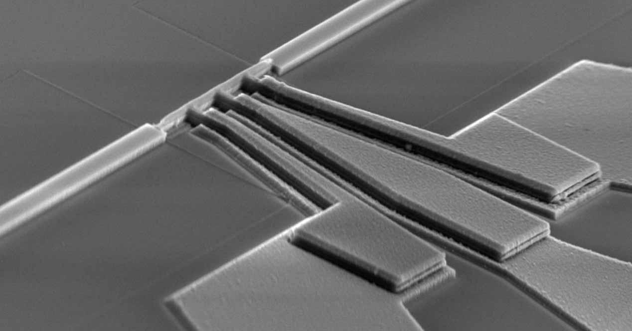
So, Toronto researchers invented a structure to take advantage of the smaller size of plasmonics and, at the same time, significantly reduce energy loss. Called a coupled hybrid plasmon waveguide (CPHW), it basically consists of a stack made up of silicon, indium, tin oxide, silicon dioxide, aluminum and more silicon. This combination forms two types of semiconductor junctions, a Schottky diode and a metal oxide semiconductor, the aluminum containing the plasmon being in common between the two. In metal, the plasmon at the upper junction interferes with that at the lower junction so that the loss is reduced by almost two orders of magnitude.
Using CPHW as a basis, two key photonic components are built: a modulator which converts electronic bits into photonics and a photodetector, which does the opposite. The modulator occupies only 2 square micrometers and can switch between states at a frequency of 26 GHz, the limit of the equipment available to researchers, but according to the measured capacity the theoretical limit would not be lower than 636 GHz.
What would this technology do?
Linking multiple processors has huge computational advantages; Imagine that we could literally have two processors running simultaneously in the system, without interfaces limiting their bandwidth. Currently it is possible to transmit up to 39 Gbps, but this technology would allow to transmit comfortably and without having to resort to error correction at 150 Gbps, so we would talk about more than four times more bits per second and all integrated in the same package, without having to resort to chiplet technology.
In short, connecting multiple processors in this way would allow us to dramatically increase the performance that a processor can offer us today, and what is more, it would allow processors to be integrated into processors almost literally, multiplying the raw performance. by two.


