Usually, the way conventional RAM has evolved has been to take advantage of newer manufacturing nodes to achieve faster memory, in bandwidth, under the same level of consumption, but with fairly smooth results.
To explain to you what the problem is with the evolution of RAM in terms of performance, bandwidth, imagine that we have an interface that transmits 1 Gb / s, which has around 64 pins and we want to expand it to support 2 Gb / s, for them we have two options:
- Double the speed of the clock.
- Double the number of pins.
The increase in clock speed causes the problem that consumption increases exponentially with clock speed and voltage and the worst thing is that in order to reach certain clock speeds the voltage has to increase so that the The increase in consumption would not be 4 times higher, but even higher so that we could run out of enough energy to power the memory.
The other option is to increase the number of pins, it means that less and less clock speed is needed, thus reducing voltage and power consumption. But the problem that this implies is that it is a matter of widening the perimeter of the chip, so that increases its cost, so if it has a better consumption solution, it is not better in terms of cost.
But the solution to this dilemma came through silicon, to connect the memory interfaces vertically on the interposer in which the processor and memory were connected, with this HBM memory was born, which allowed huge bandwidths, but with much lower power consumption.
But time goes by and HBM memory runs out of capacity because a new type of memory is needed with much lower power consumption. That’s why all eyes are on other types of memories such as fine-grained DRAM.
What is FG-DRAM?
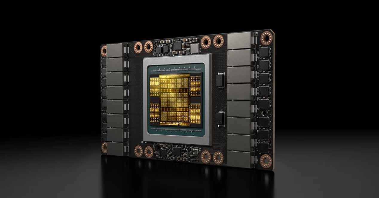
In 2017, NVIDIA made a presentation to talk about a type of DRAM called FG-DRAM or Fine Grained DRAM as a replacement proposal for HBM2, which is used in NVIDIA Tesla cards since the Tesla P100
The FG-DRAM like the HBM2 is a 2.5DIC type memory with the processor (or processors) on top of an inteposer next to the memory stacks. Its strong point? It has the particularity of going from 3.9 Pj / bit of the HBM2 memory to 2 Pj / bit, so it can offer twice the bandwidth under the same consumption as the HBM2.
From HBM2 to FG-DRAM

But Fine Grained DRAM takes a different path from what was offered with the HBM 3 in order to obtain a stack with a bandwidth of 1 TB / s. To do this, the idea is to increase the number of banks in each memory chip, up to a total of 512 simultaneous banks, accessible at a speed of 2 GB / s each.
Thanks to him. 1 TB / s FG-DRAM memory stack accessible for twice the power consumption of 256 GB / s HBM2. But since you are getting four times the bandwidth, that means consumption per transmitted bit is halved.


