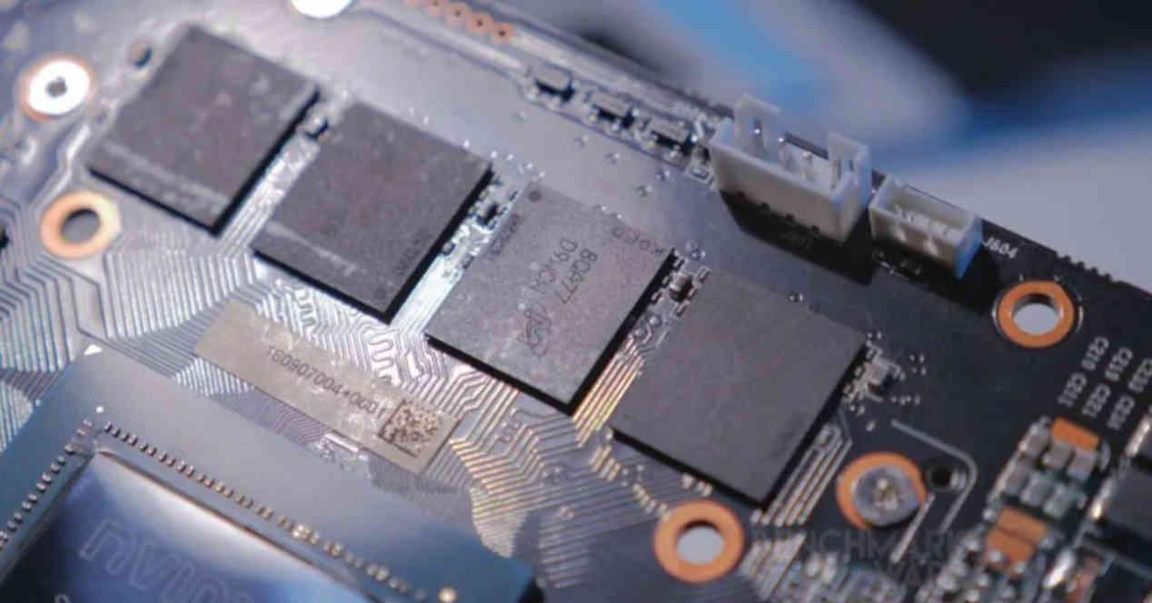
If you’ve ever wondered how low-end or mid-range graphics cards don’t have as much VRAM memory as high-end cards, this all has a very simple explanation, memory bus bandwidth affects the number of fleas. on plate, but if you want a more detailed explanation, read on.
Bus and quantity of VRAM with GDDR6 memories

If we have a GPU with a 64-bit bus, we will have two GDDR6 memory chips, if we have one with a 128-bit bus, it will be 4 GDDR6 memory chips, 192 bit 6 chip, 256 bit 8 chip, 320 bits 10 chips and 384 bits 12 chips etc.,
Obviously As the memory interface expands, the more the perimeter will occupy the GPU and the bigger it will become, For what if we want to add more capacity in the VRAM we will have to increase the memory bus, which means increasing the number of interfaces and therefore the periphery of the chip.
However, there is a mode called x8 in the case of GDDR6, which consists of two chips sharing two alternating channels, as such manner that the first chip receives the first 8 transfer bits from each channel and the other the other 8 bits to the other chip. This technique has long been used in GDDR memory and is a way to increase VRAM capacity without increasing the complexity of the memory interface, but it also does not increase the bandwidth.
This mode is used in the memory of the RTX 3090 and allows the NVIDIA card to have 24 GB of memory using 24 chips on the card, without needing a 768 bit bus for that, and yes we did. not forgot that uses GDDR6X, but does Apart from the PAM-4 interface, GDDR6 and GDDR6X work exactly the same.
Quantity of bus and VRAM with HBM memories
These memories, because they are part of a 2.5DIC setup, with an interposer in the middle and silicon vias, work differently and can appear somewhat complex.
First of all, we must keep in mind that each HBM interface is 1024 bits, but as it communicates vertically with the interposer, its interface does not occupy the perimeter space it would occupy a 1024-bit GDDR6. Of course, each interface corresponds to an HBM memory stack, the thing being:
Without interposing the HBM2 memory, this would not be possible because it is the part in charge of routing the signal to the different chips in the stack and the HBM memories do not consist of the same chip but of several different ones in the stack.

Of course, the HBM memory bus can be shortened, for example a few years ago a low cost type of HBM memory was offered with a 512 bit interface and therefore with only 2 chips per battery.
The relationship of the memory bus with the rest of the internal components of the GPU


Another relationship in a GPU is between the last level cache of it with the interfaces with the VRAM memory, as the number of partitions of the L2 increases or decreases depending on the width of the memory interface.
The last-level cache of a GPU is not only a client of the memory interface, but also previous levels of cache, some of which are located in the compute units and fixed function units such as the first one. found in raster, tessellation, or ROPS units. They are also clients of the last level cache, the command processors use the L2 cache,
Thus, the memory bus affects the number of last level cache partitions and these affect the internal configuration of the GPU.


