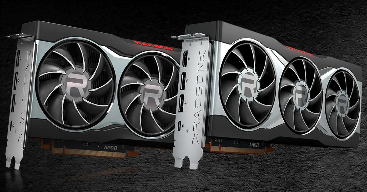
From the weeks leading up to the presentation of the RX 6000, we have known about the existence of this huge pool of memory inside the GPU, huge because we are talking about the largest cache in GPU history with a few 128 MB capacity. But AMD didn’t give much information about it, they just told us about its existence.
This is why a detailed explanation is needed to understand why AMD has placed such a large cache in its RDNA 2 version for PC.
Locating the Infinity Cache
The first point necessary to understand what is the function of a part in the hardware is to deduce its function from its location in the system.
Given that RDNA 2 is an evolution of RDNAFirst of all, we have to take a look at the first generation of the current AMD graphics architecture, of which we know two chips which are Navi 10 and Navi 14.


Well, if Infinity Cache had been implemented in RDNA, it would be in the part that says Infinity Fabric of the diagram, so at the cache organization level, we would go from this:
Where accelerators connected to the GPU Hub (the video codec, display controller, DMA players, etc.) do not have direct access to caches, not even L2 cache.
With the addition of the Infinity cache, things are already changing “a little”, since now the accelerators have access to this memory,
This is very important, especially for the Display Core Next, which is responsible for reading the final image buffer and passing it to the corresponding display port or HDMI interface so that the image is displayed at the screen, this is important in order to reduce access to VRAM by these units.
Remember the RDNA cache system
In RDNA, caches are connected to each other in the following way:
The L2 cache is externally connected to 16 channels of 32 bytes / cycle each, if we look at the Navi 10 diagram, you will see how this GPU has it 16 L2 cache partitions and a 256-bit GDDR6 bus to which they are connected.
Keep in mind that the GDDR6 uses 2 channels per chip which operate in parallel, each 16 bits.
In other words, the number of L2 cache partitions in RDNA architectures equals the number of 16-bit GDDR6 channels connected to the GPU. In RDNA and RDNA 2, each partition is 256KB, which is why the Xbox Series X which has a 320-bit bus and therefore 20 GDDR6 channels has around 5MB of L2 cache.
A new level of cache: the Infinity cache
Since this is an additional level of cache, the Infinity cache should be connected directly to the L2 cache, which is the previous level in the cache hierarchy, this is confirmed to us by AMD itself in a footer. :
Measurement calculated by AMD engineers, on a Radeon RX 6000 series card with AMD Infinity Cache of 128 MB and 256-bit GDDR6. A measure of the average AMD Infinity Cache hit rate in 4K games of 58% on top game titles, multiplied by the theoretical maximum bandwidth of the 16-channel AMD Infinity Fabric 64B which connect the cache to the graphics engine at a boost frequency of up to 1.94 GHz.
The GPU used in the RX 6800, RX 6800 XT and RX 6900 is Navi 21 which has a 256 bit GDDR6 bus, so it has 16 channels and therefore the 16 L2 Cache partitions each being connected to one Infinity Cache partition.
As for the question of success rates of 58%, it is more complicated and this is what we will try to explain below.
Caching Tiles on NVIDIA GPUs
Before continuing with Infinity Cache we need to understand the reasons for its existence and for that we need to look at how GPUs have evolved in recent years.
Starting with NVIDIA Maxwell, GeForce 900 Series, NVIDIA made a major change in their GPUs which they called Tile Caching, the change of which involved connecting the ROPS and the raster unit to the L2 cache.
With this change, ROPS s topped writing directly to VRAM, ROPS are common to all GPUs and are responsible for creating in-memory image buffers.
Thanks to this change, NVIDIA was able to reduce the energy impact on the memory bus by reducing the amount of transfers made to and from VRAM and with this, NVIDIA was able to gain energy efficiency from AMD with the Maxwell and Pascal architectures. .
DSBR, tile caching on AMD GPUs
AMD, on the other hand, for all generations of the GCN architecture before Vega, connected render backends (RBs) directly to the memory controller.
But from AMD Vega he made two architectural changes to add Tile Caching to his GPUs, the first of which was to renew the raster unit, which he renamed DSBR, Draw Stream Binning Rasterizer.
The second change was that they connected the raster unit and ROPS to the L2 cache, a change that still exists in RDNA and RDNA 2.
Usefulness of DSBR or Tile Caching
Tile Caching or DSBR is effective because it orders the geometry of the scene based on its position on the screen before it was rasterized, this was a significant change from GPUs before this technique was implemented. they sorted the already textured fragments just before sending them to the image buffer.
In Tile Caching / DSBR, what is done is sort the polygons in the scene before they are converted to fragments by the raster unit.
In Tile Caching, polygons are ordered according to their on-screen position in the tiles, where each tile is a fragment of n * n pixels.
One of the advantages of this is that it allows the non-visible pixels to be eliminated beforehand from the fragments which are opaque when they are in the same situation. Something that cannot be done if the elements that make up the scene are ordered after texturing.
This prevents the GPU from wasting time on unnecessary pixels and improves the efficiency of the GPU. In case you find it confusing, it’s as easy as remembering that throughout the graphics pipeline, the different primitives that make up the scene take on different shapes during the different stages of it.
El Tile Caching o DSBR is not equivalent to rendering tiles
Although the name can be misleading, Tile Caching is not equivalent to Tile Rendering for the following reasons:
- Tile renderers store scene geometry in memory, categorize it, and create screen lists for each tile. This process does not occur in the case of Tile Caching or DSBR.
- In tile rendering, ROPS are connected to notebook memories outside of the cache hierarchy and do not flush their content into VRAM until that tile is 100% complete, so the rates of success are 100%.
- In Tile Caching / DSBR, since the ROPS / RB are connected to the L2 cache, at any time the cache lines from L2 to RAM can be deleted, so there is no guarantee that 100% of the data is in the L2 cache.
Since there is a high probability that the cache lines will end up in VRAM, what AMD has done with the Infinity Cache is to add an additional cache layer that collects data discarded from the GPU’s L2 cache.
The Infinity cache is a victim cache
The idea of Hidden Victim It is a legacy of processors under Zen architectures which has been adapted to RDNA 2.
In Zen hearts the L3 cache is what we call a victim cache, they are responsible for collect deleted cache lines of L2 instead of being part of the usual cache hierarchy. That is, in Zen cores the data coming from the RAM does not follow the path RAM → L3 → L2 → L1 or vice versa, but rather follows the path RAM → L2 → L1 since the L3 cache acts as Victim Hidden.
In the case of the Infinity cache, the idea is save GPU L2 cache lines without having to access VRAM, which allows the energy consumed per instruction to be much lower and therefore to obtain higher clock speeds.
However, while the capacity of 128MB might seem very high, it doesn’t seem like enough to prevent all rejected rows from ending up in VRAM, because in the best case scenario he manages to save only 58%. This means that in future iterations of your RDNA architecture, it is very likely that AMD increases the capacity of this Infinity cache.
Table of Contents


