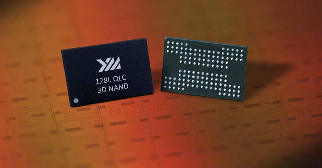
The lithography in the chips that are used in processors as we know them, they have long struggled to reduce their manufacturing processes, and we are seeing how nanometers are getting smaller and smaller. However, when it comes to memoria 3D NAND, is “stuck” in 40 nm for some time now, and the trend is for this to continue for at least the medium term. ¿Why don’t they improve lithography from memory? We’ll tell you all below.
3D NAND technology was first introduced in 2013, and Samsung did a great job of improving it in 2015; However, since then neither Samsung nor its competitors have made any further improvements to this memory beyond creating more and more layers to increase density. So if 3D NAND memory is 40nm, why don’t we see improvements with smaller nodes like 32nm, 20nm, etc.?
The answer is that it is almost impossible to reduce lithography because of the way the inter-layer communication channels are made, and we’ll explain it to you below.
This is how 3D NAND channels are made at 40nm
To explain why the lithography of 3D NAND memory cannot be much smaller, we will use Toshiba’s BiCS structure (now used by KIOXIA) as an example.
- First of all, very narrow holes are made in all layers of 3D NAND. Today these holes have an aspect ratio of around 60: 1 which is quite remarkable. Consider that for this lithograph, a one inch (2.5 inch) diameter hole would be 1.5 meters long. These holes are like that, with walls almost perfectly parallel from top to bottom which cross all the layers of matter and which serve to communicate with each other.
- These holes are then filled with great precision with 5 layers of material:
- The initial layer is silicon oxide (SiO2), which makes the hole even narrower. This is shown in pale blue in the diagram that we are going to put below.
- Then it is covered with another thin layer of silicon nitride (Si3N4) also from top to bottom, which makes the hole even narrower. This is the charge capture layer and is shown in yellow.
- There is a very thin third layer of SiO2, which makes the hole even narrower.
- The next layer is conductive polysilicon. This layer is shown in red and serves as a data transmission channel.
- Finally, the little space that remains is again filled with SiO2 (blue). This final insulating charge helps to “thin” the channel so that it functions better and is more stable.
Thus, the thickness of the layers which fill the holes determines their minimum diameter, and although we have shown it here as “large”, in reality the thickness of each inner layer is only a few atoms thick and it is practically impossible to reduce them. .
Because of this, 3D NAND memory will need to stay at 40nm for the foreseeable future, and that’s why all manufacturers’ efforts lately are to increase the number of layers that pass through these communication holes, the logic within. improved matrix and stair set-ups, but not by reducing lithography because at this point it is physically almost impossible.


