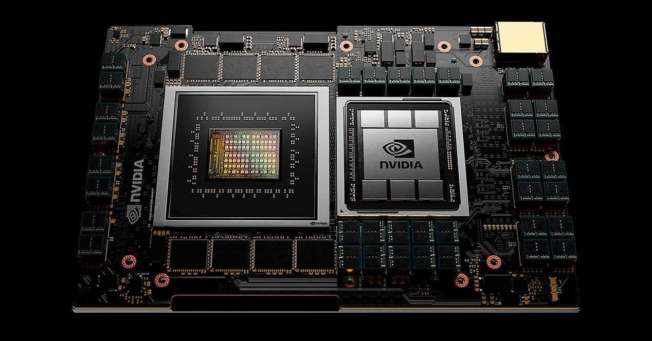
Without a doubt, what NVIDIA offers is an option halfway between Intel, AMD and even Apple, an option as smart as it is revolutionary that promises to outperform its rivals and perhaps even the charts when the two main players of the industry will launch their bets in this 2022 EPYC and Xeon are in Huang’s sights and this “new” concept could revolutionize the AI and DL industry.
NVIDIA Grace, a system more than a processor in itself
The first thing we must be clear about is that we are talking about an SoC to be used practically and not a processor as such, since being technical and specific is more faithful to reality. NVIDIA Grace is the brand blueprint for ARM and is therefore based on the N2 Perseus platform which is at the same time the first to support the ARM V9 architecture.
Note that we are talking about two SoCs differentiated by their name and their characteristics: Grace Hopper and Grace CPU SUPERCHIP
This implies at the same time more details and additional technologies, because NVIDIA has specified that the reduction of the lithographic node with the above manages to add CXL 2.0, CCIX 2.0, DDR5 and PCIe 5.0 like its rivals on computer and also HBM3. This without forgetting technologies such as C2C NVLink Chip-to-Chip with up to 900 GB/s and consistency of memory.
This is all very good and represents a giant leap forward in the industry, well ahead of what Intel and AMD currently have for the same industry, but if NVIDIA builds on Neoverse and add a whopping 72 cores in a dual configuration that make the aforementioned 144 core count, as we have a hard-to-digest bombshell for its rivals.
Concretely, the SoC is composed of these two ARM v9 chips from 72 hearts attached to a GPU Hopper connected as we said by C2C and its bandwidth, but the most impressive thing is not that in itself, but the fact that its maximum consumption is numbered at 500 watts in total for the two CPUs, a technological milestone if one takes into account the fact that they integrate SVE scalable vector instructions.
But there is more, because being a SoC it needs RAM memory, which arrives in the form of a soldered LPDDR5X and at its maximum capacity per battery, i.e. 64 GBso given the number of modules (16, eight for each chip) we have a huge 512 GB in total where thanks to C2C and improvements in the V9 architecture NVIDIA claims that the internal bandwidth has increased by 30 times no less.
A SoC with 600 GB of memory in total
NVIDIA does not add here the impressive 396 MB CPU cachebut it specifies that the bandwidth obtainable internally is 1 TB/sdouble what Intel and AMD currently earn on their EPYCs and Xeons.
As for the GPU itself, there isn’t much data and that makes sense, as it’s reserved to not give hints about desktop architectures as such.
The presentation data of the GH100 is not very precise either, quite the contrary, since it has been revealed that it is manufactured in 4 nm, it will have 144 SM distributed in 8 GPC with 48 MB of L2 and nothing else, so it’s a mystery that will be revealed in a few months.
What NVIDIA left in contention are the 80 GB of HBM3 memory, a truly impressive figure that sets a new benchmark in the sector. As for its performance, there is no data presented by the company, but there are statements as such. NVIDIA claims its Grace is 1.5 times faster than the EPYC Rome 7742 in SPECrate_2017_int_base, where it also achieves an efficiency of 250 watts per chip against AMD’s 280 watts.
Add to that the fact that NVIDIA claims Grace is compatible with RTX, IA, HPC, and Omniverse, it is certain that Intel and AMD have a strong competitor coming in the future. first semester 2023. On the other hand, and due to the specified time GAP, NVIDIA commented that there will be a technical document from Grace later, where we hope to learn more about its GPU.


