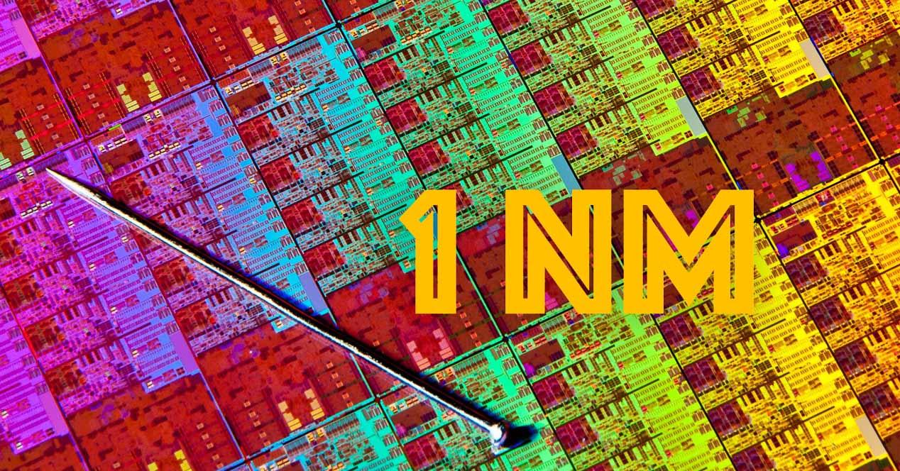
Reducing the size of the transistors is essential, but current technology is already at its limit and seems an obstacle impossible to overcome, future processors would therefore be doomed to increase in size physically in order to be able to integrate a greater number of transistors inside. . Is this the end of Moore’s Law? Is it no longer possible to overcome this obstacle? ASML and imec believe it is possible, and in fact they are so confident that they have already incorporated it into their roadmap for the next few years.
How to pass the 1nm barrier and comply with Moore’s Law
It was during the “Imec Technology Forum” (ITF) Japan 2020 that the CEO and President of imec, Luc Van den Hove, gave a keynote address to provide an overview of the company’s research process, who along with ASML (known for making wafer machines) literally state that “Moore’s Law is not going to stop”.
Van den Hove said that thanks to the new next-generation high-resolution EUV manufacturing process called High NA EUV, Moore’s Law will continue to be applied and the process will continue to be refined beyond 1nm.
Many semiconductor companies, including several in Japan, have backed out of the “race to miniaturize processes” one after another, claiming that “Moore’s Law is over” or is ” so expensive that it is not cost effective ”, but imec states that they are going to stand firm from start to finish to keep the technology moving forward, and in fact as you can see in the image below- above, they proclaim the extension of the useful life of Moore’s Law, which has become a law of truth regarding the study of component miniaturization.
When it comes to EUV exposure technology, considered indispensable for the so-called ‘ultra miniaturization’, imec has teamed up with ASML to develop a technology that allows to exceed 1nm in terms of miniaturization (however, they do not haven’t said if it will be 0.5nm, 0.9nm or what)
The roadmap for miniaturization processes
During the aforementioned conference, imec provided their roadmap (future plans) for miniaturization, from the current FinFET process to 5nm beyond 1nm (although yes they did not give any dates and not even years in the hope that these technologies are available).
If you look under the number of each of the nodes, you’ll find a series of acronyms, and they all start with PP, which is the stage of polysilicon wiring with its metrics (for example, at 3nm it’s 44 -48) while MP is the thin metal wiring pitch (following the 3nm example, it is 21-24). It should be noted that the technology node used to denote the minimum machining dimensions and the length of the logic gates, but is now a simple “label” which does not mean the actual physical length.
High NA EUV technology will allow a reduction of 1 nm
TSMC and Samsung Electronics have already introduced an EUV exposure device with NDA = 0.33 in some 7nm lithographic processes, and they are already testing with 5nm processes with this technology where they have increased in frequency. However, they have stayed there and have not given any information beyond 2nm yet. According to imec, it is necessary to achieve high resolution and high NA (NA of at least 0.55) on the exposure equipment to further reduce the size of the transistors.
ASML for its part has already completed the basic design of high exposure NA EUV equipment such as the NXE: 5000 series, but they do not expect to be able to market it until at least 2022. This new generation machine has a downside. additional, namely that it is considerably higher than the previous ones because it has a huge optical system, so manufacturers may have to adjust the ceiling height of their factories if they want to be able to put them inside.
In principle, ASML designed this machine in close collaboration with imec to go down 2nm, go down to 1nm and even exceed it, but regarding the development of the lithography process using High NA EUV equipment, Van den Hove said which follows:
“The goal of logic device process miniaturization is to reduce power (consumption), improve performance, and reduce surface area in a process we commonly call PPAC. Reducing costs, being sustainable and taking due account of the environment in addition to these four factors when moving to miniaturization below 1nm are our priorities, and it will take time to achieve this. “


