
The main question would be: why does the industry need EUV technology? Everyone migrates there, but the ordinary user doesn’t really understand what the benefits are. In short: costs, speed and scalability. Of the three, scalability is perhaps the most important as the costs and speed are not proportional and one will decrease and the other will increase, but if we have a bottleneck in scalability, the sector will not progress.
Time is intrinsically linked to speed, everyone wants to arrive sooner

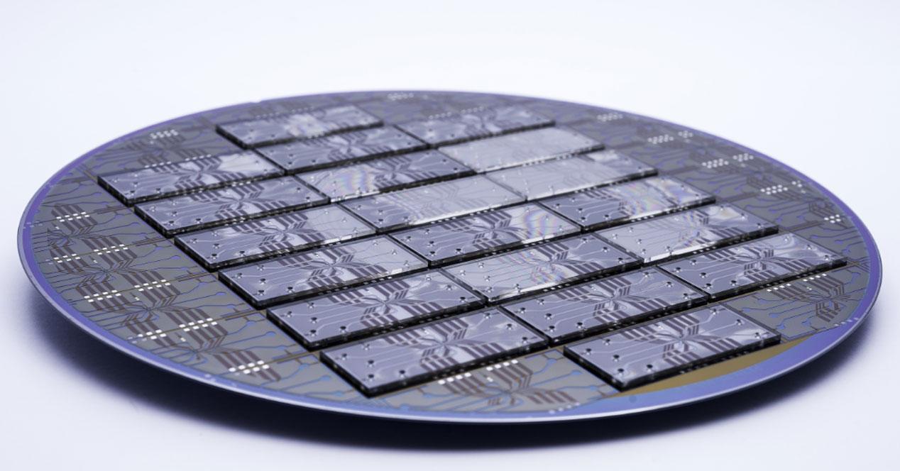
The main advantage from a mechanical engineer and lithographic mask designer perspective is that EUV simply reduces the steps and number of patterns used in each engraving.
This in itself is a key benefit, but if we also add a smaller wavelength in nanometers, we will have smaller and oddly better etched transistors to achieve more laser and scanner precision.
Because of this, TSMC, Samsung, and Intel are fighting to get ASML scanners, especially Korean, as it intends (and apparently succeeds) in including the technology in their. NAND flash for obvious reasons.
But since EUV is still a technology which is far from mature and extremely expensive, how to marry the fact that EUV is used when everything is so expensive around it? This is why all manufacturers will eventually switch to this technique …
The nature of NAND Flash allows EUV to be applied to your silicon

There are three determining factors in understanding why the industry will end up in EUVs like CPUs and GPUs. The first concerns the structure of the cells, as very regular patterns are used to create them, which implies a constant repetition of them.
The second factor is the volume involved in bringing NAND Flash to market. Since this is just a design, investing in it pays off if you don’t stop producing wafers later, and even updating the skins pays off because you improve performance and that. is still fine.
Finally, redundancy in the design allows for a higher failure rate, allowing you to make wafers and chips much more cost effective, improving the end price and being able to be competitive. If we add to that the fact that higher speeds and higher density could be achieved in these chips … we can understand why despite the huge amount of money that a scanner involves, Samsung threw itself in the door. head first in these chips.
Aren’t masks a problem for DRAM as well as CPU and GPU?

They are, for all equally, the so-called Empty space EUV masks remain a problem due to their own construction and materials. A mask consists of a light area and another dark area, where the boundaries between the two are very sharp.
The bright area is a reflector, a very thin layer 40 to 50 nanometers below the surface. The purpose of this layer is to create a reflection so that the wafer is blank at this point, so when reflecting light, an absorber is needed to acquire that light and not let it move through mirrors and c is the main problem.

If the lens and mask are not perfect enough, we will get a blurry image on the wafer and therefore the transistors will not record well. So to improve that, we use electron beams and the so-called film, a very thin layer on top of the mask which protects it from dust and any imperfections, so that the engraving is more perfect.
The use of electron beams improves precision, the film worsens it, but compensates by protecting the mask. So, the NAND Flash industry will gradually switch to EUV until in a few years all the chips are made with this currently expensive technology, so we should see very significant returns in a few years.