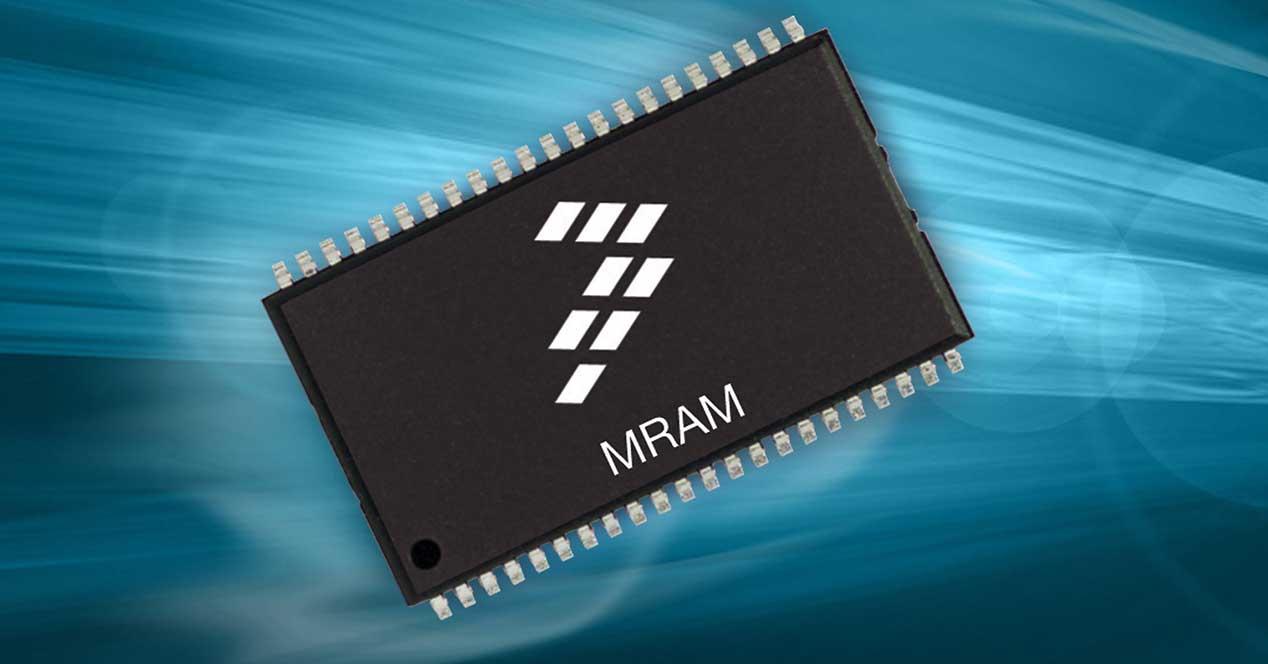
Memory (as a concept, not as a form) has suffered from a pervasive problem for years: It advances at a slower rate than the miniaturization technology of major semiconductor manufacturers. This means it’s still a link that everyone wants to skip in some way or another in their designs, but the truth is when there is no other option it becomes a problem. , and this is where MRAM comes in.
MRAM will be the chosen alternative to eFlash SRAM
There are alternatives on the market to replace traditional RAM in all its aspects like CMOS technology, towards another type of much more efficient product that adapts better and achieves more performance.
The eFlash or SRAM in its simpler versions were an option, but MRAM is the one that takes the cat to the water, since in the first each transistor is valid as cell selection and data storage, it has a high voltage and only can reduce up to 28 nm
SRAMs have cells that have between 6 and 8 transistors, they can be made to roughly the same level of miniaturization as CPU or GPU transistors, but this has a major problem – it consumes a lot of silicon, and its capacity is not high for it.
And this is where MRAM comes in, because we are talking about a type of memory that can create a storage element called a magnetic tunnel junction or MTJ by multilayer cabling or BEOL. This technology does not depend on the etching technology of the transistors
In case the concept is not clear: MRAM does not depend on the fact that we record the transistors with FinFET, FD SOI or GAA, we can do that with any of them, thus tweaking the development a lot more and launching much more precise roadmaps.
In the efficiency section, this is perhaps where it stands out the most, because since it is non-volatile access memory, the current consumption in standby mode is very low.
Three open fronts for this technology to take off for good
Samsung, IBM, Global Foundries and TSMC have already showcased their advancements with this technology in 2020, so we can get a sense of where the industry is heading and how much time remains. There are three main aspects to deal with. The first concerns the results presented at the MEI 2020 by Samsung on the fact that the MRAM can replace SRAM in a short period of time.
This is obviously very important due to the fact that half of the world market works with SRAM, the impact of which can change the paradigm of PCs and servers, among many other industries.
The second is that will replace eFlash as an integrated device, i.e. integrated MRAM. The advancement here is to have achieved a higher degree of reliability at high temperatures, so that it would already be optimal for cars, cell phones or external storage cards, among other industries. The cell retention period is said to be 1 month at over 125 ºC.
The last is the most important, because it refers to the miniaturization of technology. In two years, it went from 22nm and 40nm to more than respectable 14nm and 16nm. They are always behind the most advanced processes, but the leap is very important at all nanoscale levels.
In contrast, eMRAM has a lifespan of 100,000 cycles and a retention period of 10 years with temperatures ranging from -40 ° C to + 125 ° C, but it is only developed by GF.
What we are looking for with all these techniques is simple: integrate the logic of the current transistors into a type of memory to reduce the total surface area of the chip and thus launch a new boost to the size of the chip and the efficiency general of all SoC, CPU, APU or GPU.
It’s so advanced that Samsung is already producing this type of mass memory like eMRAM to replace Flash, so we’re not faced with future technology that might not come along, it’s a reality that everyone is trying in their fabs. to launch revolutionary products to the market.


