One of the particularities of Intel is its vertical integration where it is both designer and manufacturer of chips. This allows your architects to work closely with engineers who are dedicated to creating new manufacturing processes not only to create fully custom libraries of future nodes. For this reason, as a company, it allows them to design future processors and GPUs around these advancements.
So let’s see what technologies were presented by Intel at this year’s International Electron Devices Meeting.
Intel at the MEI 2021


There is a long time from when we start designing a processor until it reaches us for us to use it. While we’re used to seeing a continuous release rate from various manufacturers, design time can take up to five years in total and more in companies that use Full Custom libraries to design their processors, such as the company founded by Gordon Moore.
Intel at the MEI 2021 therefore spoke of the three objectives for the future, which are:
- Essential technologies for scaling: which is related to Moore’s Law and thus allows the greatest number of transistors per zone, although this requires the development of new types of 3DIC and 2.5DIC packages. As well as the use of new types of transistors.
- The second point on which they will focus is improving energy consumption in the communication of information, one of the biggest challenges today in the design of new processors.
- Creation of new concepts such as the use of new types of switches, the use of electromagnetic mechanisms or quantum computing.
All these technologies that we will talk about below, so we won’t see them in the short term in Intel’s portfolio, but they are a glimpse of what the future awaits us, both in the medium term and in the future. distant.
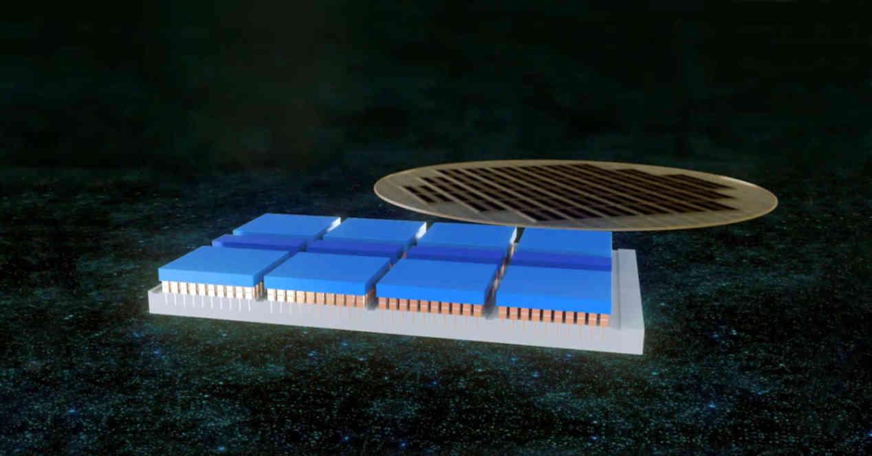
MEI 2021: Foveros Direct HBI, 3DIC and GAA

One of the keys to 3DIC packaging is the increase in the number of interconnections in the vertical connection between the chips. Since with a large number of connections, very high bandwidths can be achieved with a low clock speed and, therefore, with very low voltages.
Intel’s 3DIC intercom technology is called Foveros, which will arrive in its first generation on HPC Ponte Vecchio GPUs, while Foveros Omni and Foveros Direct, which allow up to 10,000 contacts per square millimeter, can be found on the next generation and the first of them is already being used in the development of future products, so we should expect to use both for processors under Intel node 4.

The other point related to the creation of 3DIC chips that Intel has shown in the MEI concerns the use of GAA transistors. For this, they will use their Nanoribbon technology, which will consist of NMOS and PMOS semiconductors whose gates are wound around ultra-thin channels on all four sides. Intel expects the 3DIC chip density to be between 30 and 50% higher when using transistors of this type, a much higher figure than they would get with using FinFET.
This type of transistors will not use the Intel node 4, although they will use the later manufacturing nodes and we cannot ignore that the future of CPUs and GPUs involves the creation of not only structures based on chiplets, but also on the use of 3DIC, either to communicate from logic to logic or from logic to memory.
GaN y FeRAM como eDRAM power switches

Another novelty that Intel presented at the MEI 2021 is linked to the presentation of the so-called GaN (Gallium Nitride) power switches. The work of these pieces? They are placed on PMOS transistors inside GAA gates to provide voltage. At the moment, they are designed to work in high voltage mode, so they are specially designed for built-in radio frequency.
We also cannot bypass the on-board memory implementation by using ferroelectric RAM or FeRAM. This allows the creation of memory with a density much higher than SRAM, but without the problems of DRAM in terms of speed. The speed of this memory? Well, we’re talking about latencies of 2 nanoseconds, a latency equal to that of current latencies with first-level caches.
MESO and the transition beyond MOSFET

As the entire industry studies quantum computing to overcome the limits of silicon, it’s no surprise that Intel is developing such technology that can be manufactured using CMOS technology that has been used for decades to create new processors. . .
And finally we can talk about MESO logic, which uses magnetic spins like transistors. Intel’s goal with such technology? The creation of a type of transistor located between the semiconductors of today and tomorrow and still distant quantum computers.
Of course, Intel is also conducting research in areas that have very little to do with functions that we are familiar with. These are fundamentally new techniques, such as MESO logic, which views magnetic spins as a type of transistor. This torque logic should allow entirely new methods of building a transistor, and is somewhere between current semiconductor technology and what quantum computers are implementing.
Table of Contents